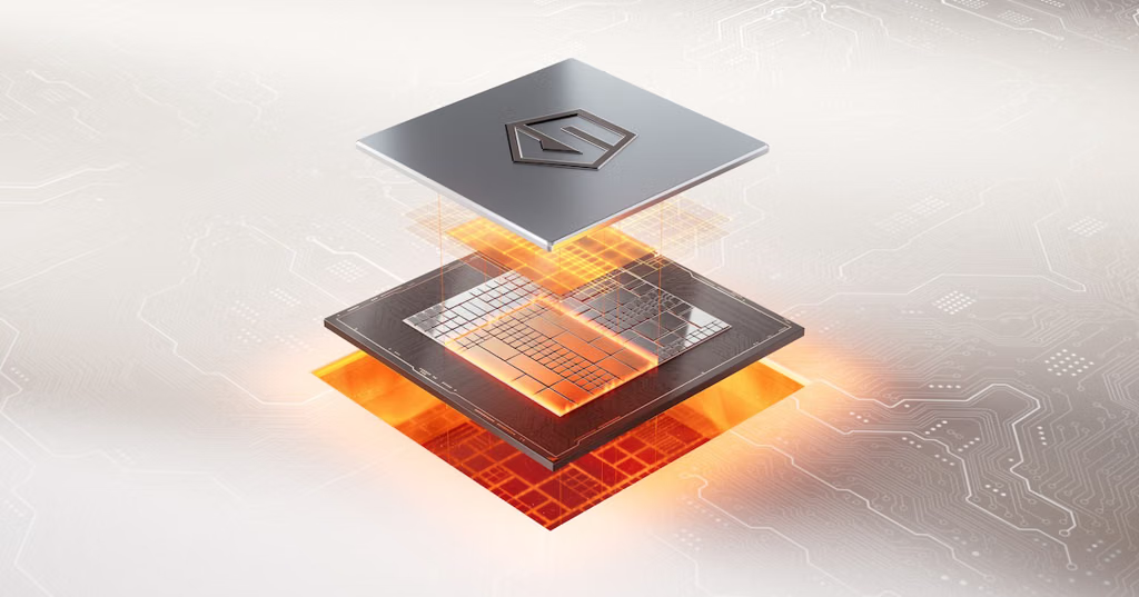
Microsoft and Google Cloud TPU are an even split for recommendations on designing custom AI silicon for workload-specific processors. Broadcom is also discussed for co-designing custom chips with OpenAI, Google, and Meta.
For an NPU evaluation, the custom AI silicon market includes several types of companies: chip architects and designers, semiconductor companies with in-house AI accelerators, and ASIC design firms that build custom chips for customers. The right shortlist depends on whether you need an edge NPU for PCs or embedded devices, an automotive processor, or a data-center AI accelerator.
A key distinction: some companies design the chip architecture and logic, while others also manufacture the silicon or provide the foundry and packaging services.
1. Companies that design custom AI silicon
These are the main companies to investigate, grouped by their role in the design process.
Custom AI ASIC co-design and implementation partners
Broadcom
(Custom ASIC)
Develops custom AI accelerators with large AI and cloud customers. A key candidate when you need a partner to co-design and implement a high-volume AI ASIC.
I need to understand the complete lifecycle of developing and manufacturing bespoke AI chips tailored to unique workloads. What does that workflow look like?
Other topics in AI Semiconductor and Accelerator Vendors
Develops custom silicon for cloud infrastructure, AI acceleration and high-speed connectivity. A relevant option for hyperscaler-scale ASIC projects.
Website:
Alchip Technologies
ASIC design and implementation partner for complex, advanced-node chips, including high-performance computing and AI accelerators.
Website:
Global Unichip Corporation (GUC)
Provides ASIC design services and implementation capabilities for advanced semiconductor projects. Worth evaluating for custom SoCs and AI silicon.
Website:
Socionext
Specializes in custom SoCs, offering a potential route for application-specific processors and embedded AI designs.
Website:
2. Companies that develop NPU and AI processor IP
These companies are relevant when you want to license an existing architecture or processor IP and integrate it into your own chip.
Arm
Offers processor IP and AI-related technologies for mobile, embedded and other devices. Particularly relevant for integrating CPU and AI acceleration into an SoC.
Synopsys has historically supplied processor IP, design software and engineering services. In January 2026, GlobalFoundries announced an agreement to acquire Synopsys' ARC processor IP business, including its NPX NPU product line; verify the transaction's closing status when assessing suppliers.
These are useful benchmarks if you're evaluating architectures, performance and software ecosystems rather than hiring an external design house.
Company
AI silicon
Primary market
Google
TPU
Cloud AI training and inference
Amazon / AWS
Trainium, Inferentia
Cloud AI training and inference
Microsoft
Maia
Azure AI infrastructure
Meta
MTIA
Recommendation and AI inference
Apple
Neural Engine
On-device AI
Qualcomm
Hexagon NPU
Mobile, PC and automotive
MediaTek
Integrated AI accelerators
Mobile and edge devices
Tenstorrent
AI accelerators and RISC-V IP
AI compute and custom silicon
The hyperscaler programs illustrate how chip architecture, workload-specific optimization and external design partnerships can work together.
4. Which companies should you evaluate first?
For an NPU project, I'd narrow the initial shortlist based on what you are trying to build:
Custom NPU ASIC from your own specifications
Start with Broadcom, Marvell, Alchip and GUC. Ask about architecture co-design, RTL, verification, physical implementation, tape-out and production support.
License NPU IP for an SoC
Start with Arm and investigate available processor IP through Cadence and Synopsys/GlobalFoundries. Compare inference throughput, power, memory architecture, supported operators and software toolchains.
Edge NPU for embedded devices, cameras or PCs
Evaluate Qualcomm, MediaTek and integrated NPU IP providers. Focus on performance per watt, SRAM requirements, quantization, model compatibility and the cost of the complete SoC.
For manufacturing, TSMC and Samsung Foundry are separate considerations: they fabricate chips rather than simply acting as interchangeable NPU architecture providers.
Apple: Integrates custom in-house Neural Engine blocks inside its A-series and M-series System-on-Chips (SoCs) to drive on-device machine learning and Apple Intelligence efficiently.[](https://www.ibm.com/think/topics/neural-processing-unit)
Qualcomm: Designs high-efficiency NPUs via its Snapdragon platforms for mobile and PC edge devices, alongside expanding custom design offerings for enterprise tech partners.
Broadcom & Marvell: Actively partner with hyperscalers to co-design and implement custom ASIC/NPU silicon solutions tailored to exact customer specifications.
Arm: Licenses fundamental processor architectures and NPU IP blocks that many other companies use as foundations to build their own custom AI silicon.
If you are evaluating NPUs for a specific deployment, are you looking at data center/cloud training/inference or edge/on-device processing , and what frameworks or workloads are you prioritizing?
Creating and producing a custom silicon accelerator—such as an Application-Specific Integrated Circuit (ASIC) or specialized Tensor Processing Unit (TPU) tailored for AI workloads like large language model (LLM) inference or computer vision—is a multi-year, multi-million-dollar engineering journey.
Workload Analysis: Profiling target AI workloads (e.g., matrix multiplications for transformers, convolution layers, specific quantization formats like F P 8 cap F cap P 8𝐹𝑃8, I N T 4 cap I cap N cap T 4𝐼𝑁𝑇4 ) to determine required arithmetic intensity and memory bandwidth.
IP and Subsystem Selection: Deciding what to build versus license—such as integrating standard host interfaces (PCIe Gen 5 5 5/6 6 6 ), high-speed memory controllers (HBM3/HBM4), and foundational processing blocks like RISC-V control cores.
Hardware Description: Translating the architecture into Register-Transfer Level (RTL) code using languages like SystemVerilog or high-level synthesis (HLS) tools from C/C++.
AI Compute Engine Design: Designing specialized processing elements, such as systolic arrays or General Matrix Multiply (GEMM) engines, optimized for low-precision parallel MAC (multiply-accumulate) operations.
Functional Verification: Using advanced verification methodologies (such as Universal Verification Methodology, or UVM) to ensure the RTL matches the architectural specification under billions of random test scenarios.
Hardware Emulation: Running the RTL on massive enterprise emulation hardware (from vendors like Siemens EDA or Synopsys ) to boot lightweight software stacks and test small AI workloads before committing to physical dimensions.[](https://siliconpatterns.com/custom-asic-design-cost-timeline-process/)
Synthesis, DFT, & Physical Design
Logic Synthesis: Translating RTL gates into a technology-specific gate-level netlist using EDA tools (from providers like Cadence or Synopsys).
Design for Test (DFT): Embedding internal test structures (like scan chains and BIST) so the physical chip can be scanned for manufacturing defects post-production.
GDSII/OASIS Hand-off: Generating the final geometric layout files (tape-out) and sending them to a semiconductor foundry (such as TSMC or Intel Foundry).
Advanced Packaging: For high-end AI accelerators, integrating the compute die with High Bandwidth Memory (HBM) using 2.5 D /3D packaging techniques like TSVs (Through-Silicon Vias) and CoWoS (Chip-on-Wafer-on-Substrate).
Compiler Infrastructure: Developing or adapting graph compilers (like TVM or MLIR-based frameworks) to map high-level AI frameworks (PyTorch, JAX) down to custom machine instructions.
Absolutely. The key idea is that a custom AI accelerator is not just a chip-design project. It is a coordinated model → architecture → silicon → compiler/runtime → system → manufacturing project. The most successful teams co-design all of those layers rather than designing hardware first and figuring out software later.
A useful mental model is:
AI workload → numerical requirements → accelerator architecture → RTL → physical silicon → compiler/runtime → deployed system → measured workload → next revision
Here is the full process.
1. Start with the AI workload, not the chip
Suppose you're building an accelerator specifically for:
transformer inference
recommendation models
computer vision
speech recognition
diffusion
graph neural networks
a particular internal AI model
First characterize the workload.
You want to know:
Compute
What operations dominate?
For example:
math
Y = XW
may mean enormous numbers of multiply-accumulate operations:
math
MAC = A \times B + C
For a transformer, you might find that the dominant operations are:
matrix multiplication
attention
softmax
normalization
activation functions
KV-cache operations
data movement
Precision
Determine whether you actually need:
FP32
BF16
FP16
FP8
INT8
INT4
binary/ternary arithmetic
Lower precision can dramatically reduce area, energy and memory bandwidth, but potentially affects model accuracy.
Memory behavior
Often the limiting factor isn't arithmetic.
It is moving data.
You therefore measure:
model size
activation size
weight reuse
cache reuse
external DRAM bandwidth
on-chip SRAM requirements
intermediate tensor traffic
Performance target
Instead of saying "make it fast," define something like:
50,000 tokens/sec at ≤100 ms p99 latency and ≤500 W.
Or for an edge device:
30 FPS object detection at <5 W.
Those constraints fundamentally determine the architecture.
2. Establish the economic case
Before designing transistors, determine whether an ASIC is justified.
You compare:
Custom ASIC
vs.
GPU
vs.
FPGA
vs.
existing AI accelerator
The ASIC has huge non-recurring engineering costs.
A simplified model is:
math
TCO = NRE + N_{chips} \times C_{chip}
where NRE includes:
architecture
RTL development
verification
EDA
IP
masks
prototypes
engineering personnel
bring-up
software
The ASIC starts making economic sense when sufficiently high volume, performance, power savings, or strategic value amortizes that investment.
This is one reason custom accelerators are particularly attractive for hyperscalers: the same silicon may be deployed at enormous scale.
3. Write the architecture specification
Now turn the workload into a hardware specification.
You define things such as:
Compute array
For example:
             Weight Memory
                  |
                  v
        +---------------------+
        |  Matrix Multiply    |
        |                     |
Input ->| PE PE PE PE PE PE   |-> Output
        | PE PE PE PE PE PE   |
        | PE PE PE PE PE PE   |
        +---------------------+
                  |
                  v
              SRAM/cache
You might choose a:
systolic array
SIMD engine
vector processor
tensor processor
spatial dataflow architecture
reconfigurable array
combination of these
Processing elements
Each PE could contain:
multiplier
     |
     v
adder ---> accumulator
Thousands of PEs may operate simultaneously.
Memory hierarchy
You decide how much data lives in:
Registers
   ↓
Local SRAM
   ↓
Shared SRAM
   ↓
HBM / DRAM
The crucial optimization is reuse.
If a weight can be reused 100 times while sitting in SRAM rather than fetched from DRAM 100 times, the energy savings can be enormous.
This is where the abstract architecture becomes an actual circuit design.
9. Verification becomes enormous
You don't simply simulate the chip once.
You need to demonstrate that it behaves correctly across an enormous number of situations.
Typical techniques include:
Simulation
Run RTL against expected results.
Formal verification
Mathematically prove properties of portions of the design.
Assertions
For example:
if request_valid == 1
then request eventually receives response
Randomized testing
Generate huge numbers of unusual sequences.
Coverage
Measure which:
lines
branches
states
functional scenarios
have actually been exercised.
Synopsys describes coverage closure, simulation, formal verification and related validation as core parts of ASIC development.
10. Create the software stack in parallel
This is one of the most important parts.
A custom accelerator is effectively useless if developers can't run models on it.
The stack often looks like:
PyTorch / TensorFlow
          ↓
       Model IR
          ↓
       Graph compiler
          ↓
   Hardware-specific
      optimization
          ↓
      Code generation
          ↓
     Runtime/driver
          ↓
        ASIC
A compiler might:
identify operators
fuse operations
quantize tensors
schedule computation
allocate SRAM
tile matrices
generate accelerator instructions
schedule DMA
synchronize compute units
This is conceptually similar to how NVIDIA TensorRT turns a model into an optimized hardware-specific inference engine. TensorRT's documented flow includes model parsing, optimization, engine generation and runtime execution.
For your ASIC, however, you're building the equivalent hardware/compiler ecosystem yourself.
11. Synthesis
The RTL is then transformed into a gate-level representation.
You tune those decisions using real performance measurements.
This is similar in principle to TensorRT's optimization approach: its builder selects optimized implementations for layers on a target device, rather than simply executing a generic model.
21. Production ramp
Once the chip is validated:
Engineering samples
       ↓
qualification
       ↓
production release
       ↓
volume wafer production
       ↓
packaging
       ↓
system assembly
       ↓
data-center / edge deployment
You establish:
manufacturing test limits
binning
reliability screening
thermal limits
firmware versions
production diagnostics
supply chain
22. Then the real optimization begins
Once thousands or millions of chips are deployed, you collect real-world data.
A concrete example: building a transformer-inference ASIC
Imagine your objective is:
Very high-throughput, low-power LLM inference.
You might discover that the workload heavily stresses:
1. Matrix multiplication
So you create a large tensor/MAC array.
2. Memory bandwidth
So you add large on-chip SRAM and perhaps HBM.
3. KV cache
So you create specialized memory-management mechanisms.
4. Quantization
You support INT8/INT4/FP8 datapaths.
5. Attention
You add specialized hardware for attention-related operations.
6. Scheduling
You create a compiler that tiles tensors to keep the compute array busy.
7. Model evolution
You make the accelerator programmable enough that a new transformer architecture doesn't immediately make the ASIC obsolete.
This last point is crucial.
A truly specialized ASIC isn't necessarily one that implements only one neural network. Often the sweet spot is:
fixed-function hardware around a programmable computational core
That gives you much of the efficiency of specialization without completely sacrificing flexibility.
Where the difficulty actually lies
People often imagine:
"Build a giant matrix multiplier."
That's actually only one piece.
The hard parts are frequently:
Layer
Core problem
Model
What computation actually matters?
Algorithm
What precision can we use?
Architecture
How do we exploit parallelism?
Memory
How do we avoid moving data?
Interconnect
How do compute units communicate?
RTL
How do we implement it correctly?
And modern chip development is increasingly computationally intensive itself; EDA vendors describe RTL simulation, implementation, circuit simulation, physical verification, library characterization and signoff as major compute workloads.
The three disciplines you ultimately have to combine
If you wanted to become capable of actually creating one, I'd divide the knowledge into three major tracks:
1. Computer architecture
Learn:
digital logic
computer architecture
parallel processors
caches/SRAM
memory systems
interconnects
SIMD/vector architectures
systolic arrays
accelerators
performance modeling
2. Semiconductor engineering
Learn:
CMOS
VLSI
RTL/SystemVerilog
synthesis
STA
floorplanning
placement/routing
DFT
physical verification
semiconductor fabrication
packaging
3. AI/compiler engineering
Learn:
neural-network architectures
quantization
model graphs
MLIR/LLVM-style compiler infrastructure
operator fusion
tiling
scheduling
memory planning
kernel generation
runtime/driver design
The intersection of those three is where custom AI silicon becomes particularly powerful.
For comparison, NVIDIA's current software stack illustrates why the hardware alone isn't the product: its inference stack spans model optimization, compilation, runtime, quantization and deployment, with different layers targeting different hardware and workloads.
One important practical distinction
There are really three different projects people call "building an AI accelerator":
Level 1 — FPGA accelerator:
You design hardware logic and deploy it on an existing FPGA. Great for learning and prototyping.
Level 2 — ASIC accelerator:
You design RTL, use an EDA flow, tape out through a foundry, and receive physical silicon.
Level 3 — Production AI accelerator company:
Everything above plus compiler, runtime, firmware, board, package, memory, manufacturing, supply chain, model support and customers.
Level 3 is where the enormous complexity—and potentially the enormous leverage—comes from.
If your goal is to understand how you could personally go from Python/PyTorch model → RTL → FPGA prototype → eventually a real manufactured AI ASIC, I can also lay out a practical 0-to-silicon learning/build roadmap, including the open-source tools and a realistic first accelerator you could build.